Breakthrough for lab-on-a-chip material

Researchers at Sweden's KTH Royal Institute of Technology have developed a new polymer suited for photostructuring, which opens new possibilities for medical diagnostics, biophotonics and 3D printing.
The so-called off-stoichiometry thiol-enes (OSTE) polymer was developed at KTH specifically to meet the need for a material suitable for both experimental prototyping and large-scale manufacturing of labs-on-a-chip—or, miniaturized bioanalytical laboratories.
"It can be very useful in a variety of applications such as near-patient diagnostic tools," says one of the developers, Tommy Haraldsson, docent in the department Micro and Nanosystems at KTH.
One of the unique qualities of OSTE polymer is that its surface is chemically reactive without adding anything or preparing the surface in a special way. Now, another benefit has been revealed.
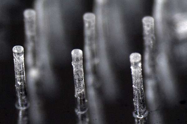
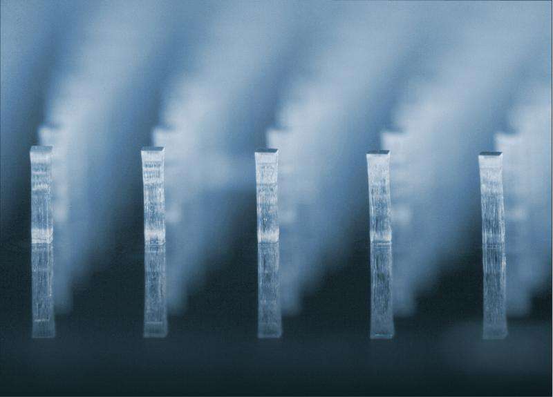
In the February issue of Nature publishing group journal Microsystems and Nanoengineering, the authors report the discovery that upon exposure to UV light, the molecules of the polymer arrange themselves in a manner that significantly enhances photostructuring.
Photostructuring is a technique by which UV light is used to solidify micro-scale 3D shapes in liquid polymer. "These microstructures can guide light, such as with waveguides. Or they can be used to control fluid flow, such as with microfluidics channels," says Gaspard Pardon, a post-doc researcher in Micro and Nanosystems at KTH.

Up until now, the major class of polymers to which the KTH material belongs, thiol-ene copolymers, has been considered to be inappropriate for photostructuring.
"With this new understanding of the underlying mechanisms and material properties available, we can also anticipate future exciting applications," Pardon says.
"Biophotonics is one such area," Pardon says. Biophotonics harnesses light and other forms of radiant energy to understand the inner workings of cells and tissues. This approach enables researchers to see, measure, analyze and manipulate biological materials in ways never before possible.
"We also started testing the 3D printing of our new material. By producing 3D structures that have the material's special surface chemical properties, it would allow the polymer to be used in a variety of new applications," he says.
The OSTE polymer was developed over the last five years to bridge the "lab-to-fab-gap", and create an alternative to suboptimal off-the-shelf materials that are now used for conceptual lab-on-a-chip device development. The predominant materials used today are known to have poor mechanical or chemical properties, such as absorption of small molecules and difficulties with permanent surface modification.
With the KTH material however it is possible to easily add different layers of material or to modify the surface properties for handling microscopic flows of fluids, without using glue or otherwise treating the material surface. Another possibility is that the material allows simple change in the surface's wettability and chemistry.
"We can also integrate sensitive biomaterials and bioreagents, and the manufacturing cost is potentially reduced because the material is so easy to work with," Pardon says.
More information: Mikael Hillmering et al. Off-stoichiometry improves the photostructuring of thiol–enes through diffusion-induced monomer depletion, Microsystems & Nanoengineering (2016). DOI: 10.1038/micronano.2015.43
Provided by KTH Royal Institute of Technology


