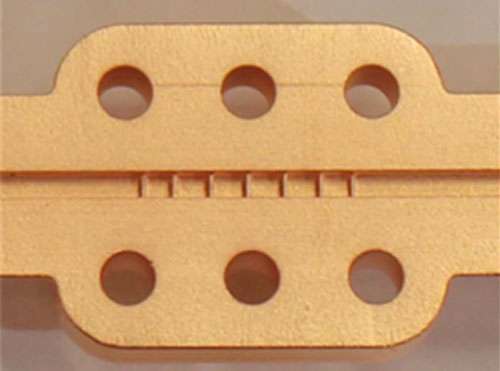
3-D printing of microwave circuits

The National Physical Laboratory (NPL) has recently assisted Imperial College London to investigate the design, fabrication and testing of waveguides manufactured using 3D-printing techniques, by providing the underpinning metrology needed to determine their electromagnetic performance.
Metallic rectangular waveguides (or waveguides, for short) are commonly used to propagate electromagnetic waves from point to point due to their relatively low-loss characteristics. They have a long history of use in many microwave applications, including radar, communications, astronomy and space. However, they can be difficult to manufacture with the precision that's needed using conventional machining techniques.
Commercial waveguides are traditionally manufactured by reshaping metal pipes through rectangular dies, or milling or erosion machining techniques, which are relatively expensive technologies. The current manufacturing cost for complex 3D structures limits potential low-cost applications; this is exacerbated in the microwave and millimetre-wave bands due to the higher precision needed for the smaller features at these shorter wavelengths.
3D-printing technology is particularly attractive for manufacturing waveguides as it allows components and circuits used at microwave and millimetre-wave frequencies to be manufactured cheaply while retaining good overall electrical performance. Since the concept of using waveguide dates back more than 100 years, this is essentially a 19th century technology fabricated using 21st century techniques.
In addition, the manufactured components are very light-weight, as they are comprised mainly of a lightweight plastic formed in a honeycomb structure. This makes them particularly attractive in applications where weight can be an issue, such as satellite payloads in space applications. However, despite the advantages of 3D-printing techniques, there seems to be little detail on the metrology needed to determine the performance of these components.
A team from Imperial College London called upon NPL's metrology expertise to help investigate the performance of two 3D-printing techniques: fused deposition modelling for microwave applications, which is a low-cost, lower-resolution technique; and stereolithography for millimetre-wave applications, which has higher resolution. To provide confidence in the results, all the measurements were performed at NPL against traceable waveguide standards.
The electrical performance of the 3D-printed waveguides was found to be comparable to standard waveguides manufactured using machining techniques - at some frequencies, the performance of the 3D-printed waveguides was actually better than conventional waveguides. This demonstrates the potential of 3D-printed waveguides as a low-cost, rapid manufacturing technology. Results from this work were published recently in IEEE Transactions on Components, Packaging, and Manufacturing Technology.
More information: "3-D Printed Metal-Pipe Rectangular Waveguides." IEEE Transactions on Components, Packaging and Manufacturing Technology DOI: 10.1109/TCPMT.2015.2462130
Provided by National Physical Laboratory


