Imaging technique for performance distribution of organic transistor arrays
Researchers in Japan have developed a new imaging technique for collective inspection of performance distribution of organic transistors. The technique drastically reduces the inspection time in the manufacturing process for information terminal devices consisting of a vast number of transistors, including electronic papers and displays.
Recent advancement in information technology and society generates a strong demand for the evolution of manufacturing technology of active backplanes which control the ON/OFF of each pixel in display devices. The most promising solution is printing-based manufacturing technology ("printed electronics" technology), because of its great advantage in manufacturing large-area devices with considerably low energy consumption. However, there has been no rapid and collective inspection technique for active backplanes consisting of a huge number of transistors, which has been a bottleneck to realize the printing-based manufacturing. In this study, the researchers developed a new gate-modulation imaging (GMI) technique which utilizes a CCD area sensor to detect tiny change of optical transmittance and reflectance of organic semiconductors induced by gate biasing of the transistors. The image obtained by this technique reflects the distribution of transistor performance, which allows rapid and collective inspection of performance distribution of organic transistors for active backplanes.
The details of this technique will be published online in a European scientific journal, Organic Electronics.
The printed electronics technology enables the production of large-area electronic devices, such as displays and sensor sheets, without the use of huge vacuum facilities and with high productivity by adopting a roll-to-roll process, so that the technology is expected to revolutionize the future electronics industry.

The practical implementation of such an innovative technology needs sophistication of elemental technologies to obtain reproducible and uniform device performance. In particular, the manufacturing process of active backplanes needs rapid and collective inspection of performance distribution for millions of transistors, so that an innovative inspection technique is strongly required.
AIST has been promoting the research and development of the printed electronics technology in a wide range of aspect. A part of the research and development has focused on a printing-based manufacturing of active backplanes and also rapid inspection of their device performance. For the inspection of active backplanes consisting of several million transistors, conventional electric measurement techniques take unrealistic time. (Assuming that the inspection of one transistor takes one minute, the total inspection time becomes about two years!) Furthermore, if we use collective inspection techniques utilized for liquid-crystalline display, it is difficult to inspect performance distribution of transistors (mobility and response time) which causes inhomogeneous brightness and display rate lowering, while defective transistors which cause dead pixels can be detected. In order to realize rapid and collective inspection of performance distribution of active backplanes, the researchers have been developed novel technique which visualizes tiny change of optical transmittance and reflectance of organic transistors induced by applying gate bias.
A part of this work was supported by the Japan Science and Technology Agency through Strategic Promotion of Innovative Research and Development Program (S-Innovation), "Development of polymer-based flexible displays: Innovation with new high-performance polymer semiconductors and their printed AM-TFTs."
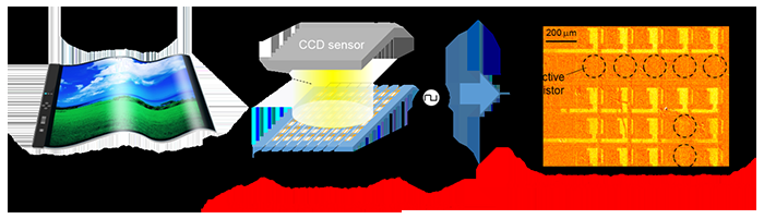
Figure 1 shows a schematic diagram of the developed GMI technique. When charge carriers are accumulated in organic transistors by applying gate bias, optical transmittance and reflectance of their organic semiconductor layer slightly change (the order of 10-4). In the GMI measurements, the gate bias is applied to all the transistors configured in the active backplane, and optical images of the transistors in the on- and off-states are captured. Then the image difference between the on- and off-states, i.e. a gate-modulation (GM) image, is obtained by image processing. The defective transistors do not appear in the obtained GM image, so that the defective transistors (and also wire disconnections) can be collectively detected.

Figure 2 shows the GM image of an organic transistor array. The yellow part corresponds to transmittance change caused by operating transistors, and the other part with no contrast corresponds to defective transistors. The intensity of the GM image shows clear correlation with transistor characteristics: high-mobility transistors demonstrate high GM intensity. This indicates that mobility distribution of transistors which causes inhomogeneous brightness of display can be collectively inspected from the intensity of the GM image.
The GM image can be obtained at various timing after the gate bias is applied to transistors, which allows examining response-time distribution of transistors. As shown in Fig. 3, transistors demonstrate gradual change from the off-state to the on-state after applying the gate bias. From the enlarged images, it was confirmed that the transistor with scratched channel demonstrates very slow response time due to its ineffective carrier accumulation. The feature enables collective inspection of response-time distribution of transistors causing display rate lowering.

The features of the developed GMI technique allow rapid and collective inspection of performance distribution of vast numbers of transistors. When a commercially-available CCD sensor with 4 million pixels is utilized for the GMI of a transistor array with 200 ppi resolution and the imaging view is assumed to be 1 cm2, the sensor can acquire a GM image of 6200 transistors by a single measurement (about 10 minutes). If high-speed CCD area sensors are configured in parallel (e.g., 400), the inspection of an active backplane consisting of more than 250 million transistors can be completed within a few minutes.
The researchers plan improvement in sensitivity and speed and imaging-area extension of the GMI technique to mount the system to practical printing-based manufacturing line of active backplanes.
More information: Reference: Organic Electronics, 25, 289-294 (2015)
Provided by Advanced Industrial Science and Technology


