High-accuracy narrow-pitch bonding of 3D ICs using thermocompression

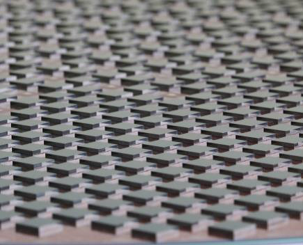
Today, at SEMICON WEST 2015 (San Francisco), world-leading nano-electronics research center imec and Besi, a global equipment supplier for the semiconductor and electronics industries announced that they have jointly developed an automated thermocompression solution for narrow-pitch die-to-wafer bonding, a method by which singulated dies are stacked onto bottom dies which are still part of a fully intact 300mm wafer. The solution features high accuracy and high throughput, paving the way to a manufacturable 2.5D, 3D, and 2.5D/3D hybrid technology.
3D IC technology, stacking multiple dies into a single device, aims to increase the functionality and performance of next-generation integrated circuits while reducing footprint and power consumption. It is a key technology to enable the next generation of portable electronics, such as smartphones and tablets, which require smaller ICs that consume less power.
One of the challenges to making 3D IC manufacturing an industrial reality is the development of a high-throughput automated process flow for narrow-pitch, high-accuracy die-to-die and die-to-wafer bonding. Thermocompression bonding (TCB) is a widespread process used by the industry for highly accurate die-to-package bonding. The method released the stress in the laminate layer and avoided stress to build up between the two stacked layers. Yet, more traditional approaches to thermocompression bonding come with long cycle times (>1 minute per die), meaning significant improvements in throughput are required to enable this stacking approach on a 300mm wafer.
Imec and Besi have developed an automated TCB process on 300 mm wafers for Besi's new 8800 TC bonder tool. Imec and Besi demonstrated die-to-wafer bonding at high accuracy, sufficient for 50 µm pitch solder micro bump arrays and a throughput of >1000 UPH with a dual bond head configuration.
"Collaborating with imec, leveraging their expertise on fine pitch bonding materials and processes, has enabled us to develop our 8800 TC bonder tool according to the needs of the semiconductor industry," said Hugo Pristauz at Besi. "This collaboration has helped us to offer our customers a viable and effective solution for 2.5D/3D IC manufacturing, especially for the new C2W applications."
Provided by IMEC


