3-D 'pop-up' silicon structures: Transforming planar materials into 3-D microarchitectures

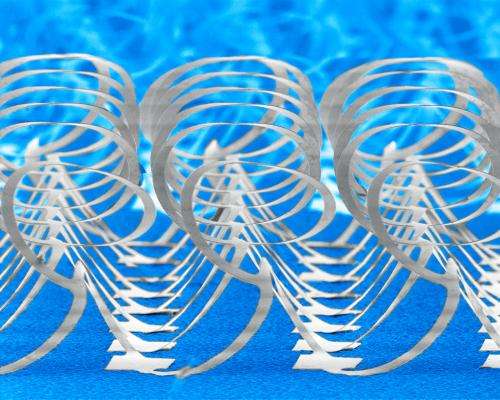
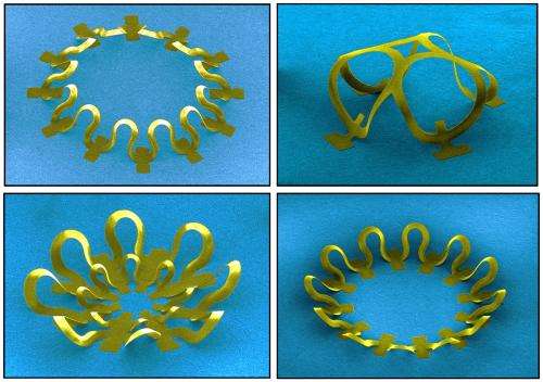
In the cover feature article of the journal, Science, researchers at the University of Illinois at Urbana-Champaign describe a unique process for geometrically transforming two dimensional (2D) micro/nanostructures into extended 3D layouts by exploiting mechanics principles similar to those found in children's 'pop-up' books.
Complex, 3D micro/nanostructures are ubiquitous in biology, where they provide essential functions in even the most basic forms of life. Similar design strategies have great potential for use in a wide variety of man-made systems, from biomedical devices to microelectromechanical components, photonics and optoelectronics, metamaterials, electronics, energy storage, and more.
Researchers noted that existing methods for forming 3D structures are either highly constrained in the classes of materials that can be used, or in the types of geometries that can be achieved.
"Conventional 3D printing technologies are fantastic, but none offers the ability to build microstructures that embed high performance semiconductors, such as silicon," explained John Rogers, a professor of materials science and engineering at Illinois. "We have presented a remarkably simple route to 3D that starts with planar precursor structures formed in nearly any type of material, including the most advanced ones used in photonics and electronics. A stretched, soft substrate imparts forces at precisely defined locations across such a structure to initiate controlled buckling processes that induce rapid, large-area extension into the third dimension. The result transforms these planar materials into well-defined, 3D frameworks with broad geometric diversity."
"The 3D transformation process involves a balance between the forces of adhesion to the substrate and the strain energies of the bent, twisted elements that make up the planar precursors," explained Sheng Xu, a postdoctoral fellow and co-author of the research paper. "Basically, we print 2D structures onto a pre-strained elastomer substrate with selected bonding points. Releasing the substrate to its original shape induces buckling processes that lift the weakly bonded regions of the 2D structure out of contact with the surface. The resulting spatially dependent deformations occur in an ordered sequence to complete the 3D assembly."

These motions follow precisely the predictions of 3D computational models of the mechanics. These models, in turn, serve as rapid, inverse design tools for realizing a wide range of desired shapes. Compatibility with the most advanced materials (e.g. monocrystalline inorganics), fabrication methods (e.g. photolithography) and processing techniques (e.g. etching, deposition) from the semiconductor and photonics industries suggest many possibilities for achieving sophisticated classes of 3D electronic, optoelectronic, and electromagnetic devices.
"With this scheme, diverse feature sizes and wide-ranging geometries can be realized in many different classes of materials," stated postdoctoral fellow and co-author Zheng Yan. "Our initial demonstrations include experimental and theoretical studies of more than forty representative geometries, from single and multiple helices, toroids and conical spirals, to structures that resemble spherical baskets, cuboid cages, starbursts, flowers, scaffolds, fences and frameworks, each with single and/or multiple level configurations, constructed in various materials, including semiconductors, conductors and dielectrics."
"This work establishes the concepts and a framework of understanding. We're now exploiting these ideas in the construction of high performance electronic scaffolds for actively guiding and monitoring growth of tissue cultures and networks for 3D electronic systems that can bend and shape themselves to the organs of the human body. We're very enthusiastic about the possibilities." Rogers added.
With his research teams, Rogers has pioneered flexible, stretchable electronics, creating pliable products such as cameras with curved retinas, medical monitors in the form of temporary tattoos, a soft sock that can wrap an arrhythmic heart in electronic sensors, and LED strips thin enough to be implanted directly into the brain to illuminate neural pathways. His work in photovoltaics serves as the basis for commercial modules that hold the current world record in conversion efficiency.
More information: "Assembly of micro/nanomaterials into complex, three-dimensional architectures by compressive buckling," www.sciencemag.org/lookup/doi/ … 1126/science.1260960
Journal information: Science
Provided by University of Illinois at Urbana-Champaign


