Researchers develop powerful, silicon-based laser

A silicon-based laser that lases up to a record 111°C, with a threshold current density of 200 A/cm2 and an output power exceeding 100 mW at room temperature, has been demonstrated by collaborating researchers from University College London (UCL) in the UK, and University of Arkansas in the US. This work could permit the creation of complex optoelectronic circuits, enabling chip-to-chip and system-to-system communications on Si substrates.
"Our demonstration of laser operation at temperatures over 100°C indicates that our III-V materials grown on silicon substrates are as good as those grown on native substrates," said Dr Siming Chen from UCL, the lead author in this work. "The ability to grow III-V materials on the whole Si substrate and then fabricating it to provide electrically pumped lasers makes mass-production possible."
The laser challenge
With silicon-based electronics reaching its limits, silicon photonics, which combines the advantages of photonics and electronics, has been under intense development over the last 30 years as a technology to create ultra-fast optical data processing. Rapid progress has already been made in developing Si-based modulation and detection technologies and most of the passive components are now at a stage where they can be used.
Si lasers, on the other hand, have not been achieved, because Si is an indirect bandgap material and the process of accomplishing efficient irradiative recombination is naturally inefficient. The requirements for an electrically pumped laser to lase are much more challenging than for an optically pumped laser, but the market importance is much greater, as an electrically pumped laser enables monolithic integration of the laser with electronics, and no need for off-chip optical sources.
According to Chen, the Si laser is "now considered to be the holy grail of Si photonics because of the technical challenge, the applications importance and the market value of lasers among all the Si-based photonic components."

A layered approach
III-V lasers grown on III-V substrates are well established as high-performance lasers, and an attractive solution to overcome the problems with Si lasers is to fabricate a III-V laser on a Si substrate. However, this has its own challenges in that there is a large lattice mismatch and difference in expansion coefficients of the two materials that causes high-density threading dislocations to form, which deteriorate the lasing performance.
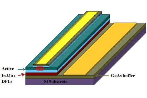
A few years ago, the UCL team were the first to demonstrate the operation of an electrically pumped InAs/GaAs quantum-dot laser epitaxially grown on a Si substrate. This was achieved using InGaAs/GaAs strained layer superlattices as dislocation filter layers to reduce the density of the threading dislocations.
The team have since been working on optimising this buffer layer, and have achieved a higher performance by using InAlAs/GaAs. In their latest work, presented in this issue of Electronics Letters, they demonstrate the highest lasing temperature for InAs/GaAs QDs lasers directly grown on Si substrates.
"While modern silicon electronic chips often work at 65°C or above, measured by an on-chip thermal coupler, the actual temperature of the transistors may be higher," said Chen. "As our laser is designed for silicon photonics, it is vital that lasers can work at a high temperatures. Our Letter demonstrates quantum dot lasers monolithically grown on a silicon substrate that can work efficiently at the same temperature as the electronic devices. In this aspect, the work is in advance of all other approaches to fabricate lasers on silicon substrates."
Future development
The team will continue to further optimise the III-V buffer layers to minimise the crystal imperfections, which will increase the laser performance, and also improve reliability.
"We have already seen that researchers worldwide are adopting the approaches we have pioneered," said Chen. "Our goal is to demonstrate a photonic transceiver circuit monolithically integrated with electronic circuits. In the long term, we are trying to work with more industry partners on this growth platform to minimise the barrier between research demonstration and industrial application."
Over the next decade, the researchers expect to see the realisation of III-V quantum dot lasers, monolithically integrated on Si, with a performance and operating lifetime approaching the state of the art GaAs- or InP-based lasers operating at optical communications wavelengths.
"Given the increasing interest in this field and the urgent demand for high performance Si-based light sources, commercial-grade Si-based III-V QD lasers should be achieved in the next decade," said Chen.
More information: "1.3 μm InAs/GaAs quantum-dot laser monolithically grown on Si substrates operating over 100°C" S.M. Chen et al. Electronics Letters, Volume 50, Issue 20, 25 September 2014, p. 1467 – 1468. DOI: 10.1049/el.2014.2414
Journal information: Electronics Letters
Provided by Institution of Engineering and Technology


