'Greener,' low-cost transistor heralds advance in flexible electronics
As tech company LG demonstrated this summer with the unveiling of its 18-inch flexible screen, the next generation of roll-up displays is tantalizingly close. Researchers are now reporting in the journal ACS Nano a new, inexpensive and simple way to make transparent, flexible transistors—the building blocks of electronics—that could help bring roll-up smartphones with see-through displays and other bendable gadgets to consumers in just a few years.
Yang Yang and colleagues note that transistors are traditionally made in a multi-step photolithography process, which uses light to print a pattern onto a glass or wafer. Not only is this approach costly, it also involves a number of toxic substances. Finding a greener, less-expensive alternative has been a challenge. Recently, new processing techniques using metal oxide semiconductors have attracted attention, but the resulting devices are lacking in flexibility or other essential traits. Yang's team wanted to address these challenges.
The researchers developed inks that create patterns on ultrathin, transparent devices when exposed to light. This light sensitivity precludes the need for harsh substances or high temperatures. "The main application of our transistors is for next-generation displays, like OLED or LCD displays," said Yang. "Our transistors are designed for simple manufacturing. We believe this is an important step toward making flexible electronics widely accessible."
More information:
"Direct Light Pattern Integration of Low-Temperature Solution-Processed All-Oxide Flexible Electronics" ACS Nano, 2014, 8 (9), pp 9680–9686
DOI: 10.1021/nn504420r
Abstract
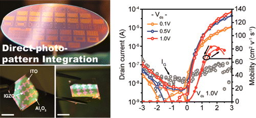
The rise of solution-processed electronics, together with their processing methods and materials, provides unique opportunities to achieve low-cost and low-temperature roll-to-roll printing of non-Si-based devices. Here, we demonstrate a wafer-scale direct light-patterned, fully transparent, all-solution-processed, and layer-by-layer-integrated electronic device. The deep ultraviolet irradiation of specially designed metal oxide gel films can generate fine-patterned shapes of ∼3 μm, which easily manifest their intrinsic properties at low-temperature annealing. This direct light patterning can be easily applied to the 4 in. wafer scale and diverse pattern shapes and provides feasibility for integrated circuit applications through the penetration of the deep ultraviolet range on the quartz mask. With this approach, we successfully fabricate all-oxide-based high-performance transparent thin-film transistors on flexible polymer substrates.
Journal information: ACS Nano
Provided by American Chemical Society


