Optics: A step in time saves two

A technique that reduces the time to simulate the operation of active optical devices aids the design of nanoscale lasers.
Tiny optical components—the heart of modern communications systems—might one day increase the operational speed of computers. When designing these components, optical engineers rely on mathematical simulations to predict the performance and efficiency of potential devices. Now, Qian Wang at the A*STAR Data Storage Institute and co?workers have developed a neat mathematical trick that more than doubles the speed of this usually slow computation1. Their method also enables more accurate modeling of increasingly complicated structures.
In the mid-nineteenth century, the physicist James Maxwell established a set of equations that describe the flow of light. The oscillating electric and magnetic fields of an optical pulse react to the optical properties of the medium through which it is travelling. "Combining Maxwell's equations with equations that describe light–matter interactions can provide a powerful simulation platform for optoelectronic devices," explains Wang. "However, running the computations is usually time-consuming."
Finite-difference time-domain (FDTD) simulations are a well-established method for modeling the flow of light in optical devices. This technique models a device as a grid of points and then calculates the electric and magnetic fields at each position using both Maxwell's equations and knowledge of the fields at neighboring points. Similarly, calculating the time evolution of light using Maxwell's equations is simplified by considering discrete temporal steps. Smaller spatial and temporal steps yield more accurate results but at the expense of a longer calculation time.
Electron density in a semiconductor is a key determiner of a material's optical properties. This density varies at a slower rate than the electric and magnetic fields of the optical pulse. Wang and his colleagues therefore eliminated calculation of this material property at every time step to shorten the calculation.
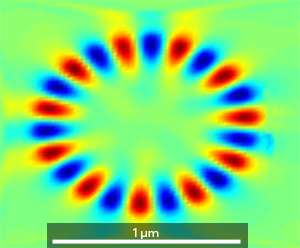
The researchers proved the usefulness of their approach by modeling a semiconductor laser, consisting of a cylindrical cavity 2 micrometers in diameter that traps light at its edges (see image). The trapped light supplies the optical feedback required for lasing. They simulated the operation of this device using an FDTD spatial grid with a 20-nanometer resolution and 0.033 femtosecond time steps. The calculated field pattern in the cavity was the same whether the active optical properties of the semiconductor were calculated at every time increment, or once every 100 steps. Yet, this simplification reduced the computation time by a factor of 2.2.
"Currently we are applying our approach to design integrated nanolasers as a next-generation on-chip light source for various applications," says Wang.
More information: IEEE Photonics Technology Letters 24, 584–586 (2012). doi: 10.1109/LPT.2012.2183865


