May 29, 2013 feature
CNT wrap-gate transistors could extend transistor performance scaling

(Phys.org) —Throughout the '70s, '80s and '90s, transistor performance continually increased according to some simple scaling rules. These rules postulate that transistor size and supply voltage should decrease as power density remains constant, resulting in an overall increase in performance. However, physical limitations stopped supply voltage scaling in the early 2000s, so the simple scaling rules no longer apply. Now any increase in performance comes at the cost of an increase in power consumption, so that transistor performance has leveled off since the mid-2000s.
Now in a new study, researchers at the IBM T.J. Watson Research Center in Yorktown Heights, New York, have harnessed the potential of carbon nanotubes as a way to extend the scaling rules and achieve further performance improvements in transistors. One day, transistors made of carbon nanotubes may form the backbone of many of our electronic devices, including smart phones and tablets.
The scaling interruption that transistors encountered in the last decade was largely due to the physical characteristics of the transistors themselves, which are silicon metal-oxide-semiconductor field-effect transistors (MOSFETs). In the past few years, researchers have investigated the possibility of replacing MOSFETs with carbon nanotube field-effect transistors (CNTFETs). These transistors have already demonstrated many attractive characteristics, including good performance at low voltages with channel components of less than 10 nm in length—a scale that silicon MOSFETs cannot physically reach with good performance.
"There are two foremost reasons why CNTFETs provide benefits that MOSFETs cannot: 1) The CNTs are ultrathin-body semiconductors (~1 nm), which allows them to be integrated into aggressively scaled devices without losing control over the current in the channel; and 2) CNTFETs can operate at low supply voltages, meaning they can provide the level of electrical current needed to drive integrated circuits at less voltage than MOSFETs can ever achieve," coauthor and IBM researcher Aaron D. Franklin told Phys.org. "For nearly a decade, there has been little to no reduction in the supply voltage for MOSFET technologies—CNTFETs are one of the best options for changing that trend."
However, to compete with MOSFETS, CNTFETs still require several major advances, including a scalable gate that can self-align to the source and drain contacts, complementary n- and p-type devices (which differ due to polarization), and compatibility with the wire processing needed to build circuits.
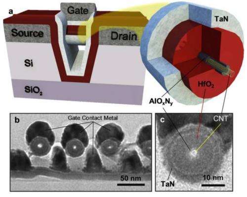
In their paper, the researchers have met all three of these requirements by building a CNT transistor with a gate that completely surrounds the CNT channel. The researchers explain that this gate-all-around (GAA) geometry is ideal because it protects the CNT from coupling to neighboring CNTs and from stray charges that come too close on such a small scale and cause instability.
"The greatest significance of this work is the implementation of a gate that completely wraps the cylindrical CNT channels," Franklin said. "Because nanotubes are just single molecules of ~1 nm diameter and are made from a single shell of atoms (hollow on the inside), they are very sensitive to electrical perturbations in their vicinity. By wrapping each CNT channel in its own dielectric and metal gate, they become isolated from such perturbations and take the devices one step closer to a reproducible and reliable technology."
The wrap-around gate is also self-aligned with the source and drain contacts without requiring lithography. As a self-aligned gate, it does not overlap or underlap the source/drain, but fits nearly perfectly, which is important for ensuring a good path for charge flow. The researchers could also scale the gate length down to 20 nm, and predict that further scaling is possible for even smaller CNT channels.
The gate can also be used to realize both n- and p-type devices by using different dielectric materials to change the polarity. Although the n-type device has a better performance than the p-type device, the researchers predict that the latter could be improved by making thinner spacer regions, since these spacers create a barrier to charge transport.
The researchers also performed quantum simulations of the CNTFET to confirm their understanding of the device's operation. The simulation results closely matched the experimental results, and also allowed the researchers to project the impact of different variables on device performance, including spacer thickness and doping. These modifications could theoretically increase the on-current, decrease the off-current, and deliver a subthreshold swing very near the theoretical limit of 60 mv/dec, which means the transistor can switch very quickly between the on and off states.
Going forward, the results demonstrate that arrays of CNTs can be integrated into scalable, self-aligned n- and p-type transistors with ideal wrap-around gates. The researchers predict that, with further optimization, these CNTFETs could one day serve as low-voltage, high-performance transistors that have a widespread impact on future applications.
"At IBM, we have shown in the past few years that you can achieve excellent CNTFET performance down to sub-10 nm channel lengths and now can do so in a technologically compatible wrap-gate structure," Franklin said. "The greatest challenge remaining at the device level is to improve the injection of carriers at the metal-CNT contacts of the devices. When contacts are scaled to the needed small dimensions for a technology, the contact resistance rises substantially and must be addressed. While this problem is not unique to CNTFETs (MOSFETs of all type suffer similarly), it is an obstacle that requires a resolution in order to access the full potential of a CNT technology.
"Outside of the device area, the two major materials hurdles are to continue increasing the purity and isolation of semiconducting CNTs from their metallic counterparts and to precisely assemble the CNTs into precise locations on a substrate. Both of these areas have seen impressive progress in the last year, both from IBM and other research groups."
More information: Aaron D. Franklin, et al. "Carbon Nanotube Complementary Wrap-Gate Transistors." Nano Letters. DOI: 10.1021/nl400544q
Journal information: Nano Letters
© 2013 Phys.org. All rights reserved.


