Researchers open door to advanced molecular electronic metrology

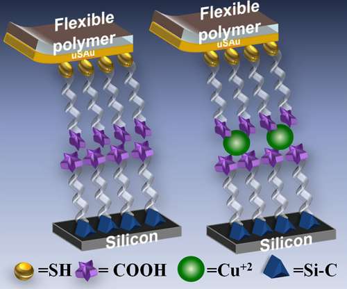
(Phys.org) —Continued advancements using a NIST-developed molecular-level fabrication technique are leading to new discoveries in the metrology for molecular electronics by advancing large-area (μm to mm range) connections to molecules (nm range). Researchers in the PML's Semiconductor and Dimensional Metrology Division have been able to build a simple bilayer molecular circuit, combining separately formed monolayers of organic materials on silicon and gold surfaces respectively to create a fully characterized molecular level device. Further, they were able to place copper atoms at specific locations within the bilayer device to test their influence on its electronic properties.
Incorporating molecular-based materials and elements into electronics has been of great interest because of the potential applications such as memory-based devices, organic thin-film transistors, and spintronic devices. The incorporation of organic monolayers with silicon is advantageous from a technological manufacturing point of view because of the extensive manufacturing infrastructure that would allow for rapid integration with Si-based CMOS technologies. Moreover, the molecular layer can be used to engineer and alter the surface energetics of the semiconductor.
"We're trying to miniaturize electronics," explains Christina Hacker, leader of the Nanoelectronic Device Metrology Project. "We can't really shrink existing transistors too much more. So, we're reaching the scale where we're looking for different ways of doing computing. With molecular electronics, you're looking at either a single monolayer or a single molecule and trying to understand how that molecule behaves in an electronic fashion."
"Organic molecules can actually serve different functions that a metal can't," Hacker continues. "A metal is going to be a conductor. A metal-oxide is going to be an insulator. A molecule could be something different. It could act as a switch. It could also change the work function of the system as a whole. You could have different properties when you put that molecule in there that couldn't have with just a metal or just an oxide."
Creating a test structure to enable measurements of organic molecular-level devices, however, has been a challenge. Previously, PML researchers solved the metrology bottleneck of how to put electrodes onto molecular layers without damage with a technique they invented and termed flip-chip lamination (FCL).1
"One of the challenges with molecular electronics is actually making the contact to the molecules," Hacker explains. "Molecules are very sensitive. You can think of molecules as kind of like lettuce—if you put hot metal on lettuce, bad things happen."

Using FCL, the ultrasmooth, large area electrodes and optimized molecular monolayers are formed separately and fully characterized prior to the fabrication of the solid-state molecular electronic test structure. This provides stable devices of known nm scale structure necessary for proper metrology of the electronic function. After each layer has been characterized, they are brought together like the world's smallest sandwich.
Recently, PML researchers have succeeded in taking this FCL technique a critical step forward by making large area solid-state molecular electronic test structures from molecular bilayers and incorporating electrochemically active metal ions.2

"Before, we'd been able to do it with one layer, but we hadn't been able to do it with two molecules," Hacker explains. The new work provides a first-of-its-kind holistic snapshot of the electronic properties of molecular monolayers, bilayers, and atomic scale metal-molecule hybrids.
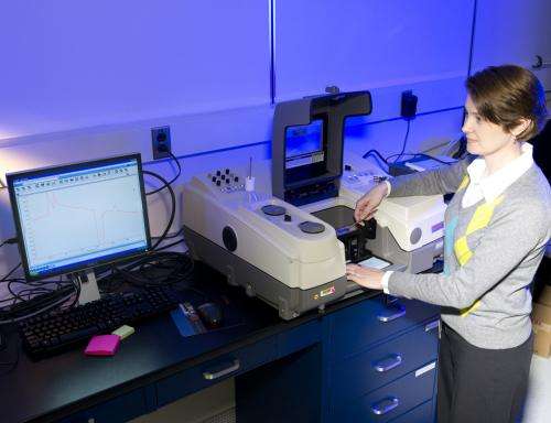
Hacker and her staff created the bilayers by self-assembing organic monolayers onto ultrasmooth layers of gold by using thiol chemistry and then bonded them to molecular layers that were reacted onto n-type silicon. This process created a silicon/molecular bilayer/metal junction, chemically sandwiching a molecular bilayer between silicon and gold electrodes. Prior to junction formation, the monolayers were physically characterized by using polarized infrared absorption spectroscopy, X-ray photoelectron spectroscopy, and near-edge X-ray absorption fine structure spectroscopy, confirming the molecular quality and functional group termination.
"We started from two pristine surfaces, one being gold and one being silicon, and then made monolayers on them," Hacker describes. "Bringing them together, we made a very high quality bilayer junction. Then, we were able to make bilayer junctions with copper in the middle and look at the function of how that copper, which is an electrically active ion, affects the electronic properties of the molecular junction as a whole. It turns out that it didn't, which was a bit of a surprise. We expected that it would."
"We saw an electrochemical connection," Sujitra Pookpanratana, Hacker's colleague, elaborates, "but those effects didn't propagate into a difference in electronic measurements of the completed bilayer device." This uncovers the unique challenge in the field of molecular electronics: Materials don't necessarily behave as previous research would indicate once they are scaled down to the molecular level. "It does change the way of thinking for molecular electronics," Pookpanratana states. "Based on previous research we think it should go in one direction, but in the end it might not propagate into the electronic properties that we'd hoped for."
Surprises were also found in the devices' current, which remained at the same level after a certain length despite increased distance from the charge source. This, Hacker and Pookpanratana believe, is due to the current transitioning to a different electron transport regime. So, despite huge advancements in the field, there is still much to learn about predicting the electrical properties.
"One of the fundamental metrology questions we have is, if we know this structure exists – that is, we know we have a bilayer and we know it's attached to electrodes in this fashion – if we were to try to predict what the electronic function would be, could we do it?" Hacker states. "Still, we are a long way away from doing that, because there are so many different things that really affect the electronic function."
Having expanded the utility of FCL to develop more complex molecular-level devices than ever before available, PML is paving the way for the future design and engineering of complex molecular electronic devices that will incorporate different molecules or materials for added device functionality and capabilities. These devices will help answer important metrology questions about electronic properties and continue to help advance the field.
More information: Coll, M. et al. Formation of Silicon-Based Molecular Electronic Structures Using Flip-Chip Lamination, Journal of the American Chemical Society, Vol. 131, pp. 12451-12457 (11-Aug- 2009).
Pookpanratana, S. et al. Electrical and Physical Characterization of Bilayer Carboxylic Acid Functionalized Molecular Layers, The Journal of Physical Chemistry C, Vol. 29, No. 6, pp. 2083-2091 (30-Jan-2013).
Journal information: Journal of the American Chemical Society , Journal of Physical Chemistry C
Provided by National Institute of Standards and Technology


