Designing materials for the future

As energy demands rise, materials scientists are increasingly interested in developing longer-lasting materials for use in the next generation of advanced nuclear and fusion reactors. However, before researchers can think about the big picture, they have to see what's happening with these materials on the atomic level.
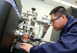
One way to do this is to use atom probe tomography (APT), a sophisticated microscopy technology, to zoom in on a material's basic building blocks. In about an hour, APT can characterize millions of atoms, telling researchers what kinds of atoms are present and pinpointing the location of each one. This sort of detailed information improves scientists' understanding of how materials are structured and gives them greater insight into how the properties of these materials can be manipulated and optimized.
In 1986, Michael Miller of ORNL's Materials Science and Technology Division was among several researchers who invented the first instruments capable of doing APT. Today, he's using this technique to study nanoclusters in nanostructured ferritic alloys, a subclass of steels that is being considered for use in next-generation nuclear power applications. The microstructures of these materials will tolerate temperatures of 1000° Celsius and radiation levels well beyond those present in today's nuclear reactors.
Ferritic alloys are expected to provide the first line of defense around nuclear reactor cores, protecting the rest of the reactor from radiation damage. To accomplish this, the alloys need to remain stable in a hostile, extreme-radiation environment. Miller has discovered that the materials best able to provide this stability are those containing chromium for oxidation resistance; titanium, yttrium and oxygen to form nanoclusters; and chromium and tungsten to segregate the grain boundaries.
"Due to their high density of nanoclusters, nanostructured ferritic alloys are one of the most stable iron-based systems materials scientists have discovered so far," Miller says. "However, there's still much to learn about nanoclusters, such as precisely how they tolerate extreme doses of radiation."
APT has revealed that some of the nanoclusters are located in the interiors of the grains and some on the grain boundaries of nanostructured ferritic alloys. This positioning is critical to the durability of the alloys. Under stress, atoms in steel alloys tend to move from grain to grain, causing the grains to grow, which results in deformation of the steel and degradation of its mechanical properties. When nanoclusters are located at the grain boundaries, however, they minimize this movement of atoms and stabilize the structure of the steel. Nanoclusters also provide stability by dispersing potentially damaging helium bubbles, which can form along grain boundaries in a nuclear reactor environment.
Understanding a material's structure helps Miller determine how to change its characteristics. For example, it's common to insert obstacles, such as nanoclusters and precipitates, into a material's crystal lattice to strengthen it. "It's like the story of Goldilocks," Miller said. "You have to find and insert just the right number of obstacles into the material. Too many obstacles and the material becomes brittle, too few and the material may not have enough strength for the application; so it's crucial to introduce the appropriate amount and for them to be stable under extreme conditions."
A suite of techniques
To study nanostructured ferritic alloys, Miller uses a combination of APT and electron microscopy. Miller and his coworkers conduct APT and electron microscopy research at ORNL's Shared Research Equipment (SHaRE) User Facility, which houses the local electrode atom probe (LEAP), the laser-assisted LEAP, a dual-beam focused ion beam (FIB)/scanning electron microscope system, and several electron microscopes.
APT requires a needle-shaped specimen with a tip that is sharp even by nanoscale standards. Miller uses an electropolishing system and the dual-beam FIB system to create his specimens. "This system focuses two beams on one spot," he says. "The electron beam shows me what I'm doing, and the ion bean sputters material away from the specimen in a precise way." Miller can "cut out" a 10-micron-long block this way, then "pencil sharpen" the block into a needle with an end radius of about 50 nanometers. Once Miller has fashioned his specimen, he characterizes the nanoclusters by stripping atoms off the surface one at a time so they fly down a time-of-flight mass spectrometer to a single-atom, position-sensitive detector. The resulting data enables Miller to identify the type of atom and where it was located in the sample. He uses this information to determine the size, number density, distribution, and composition of the nanoclusters in the materials he is studying.
This process allows the APT to produce three-dimensional images of the internal structure of metals and semiconductors by reconstructing millions of two-dimensional slices, each containing a few atoms. Unlike some other analytical techniques, APT also sees all of the elements, without restrictions, allowing Miller and his staff to determine the complete composition and microstructure of materials at the atomic level. Finding tiny nanoclusters can be difficult, but APT detects particles down to a size of five atoms—about one hundred thousand times smaller than the diameter of a human hair.
Room for advancement
Despite advances made in APT in the past 25 years, Miller says there's still room for improvement. "We're always after higher resolution," he said. "We're also interested in improving our ability to determine the position of atoms."
All of these techniques and atomic-scale characterizations will help materials scientists develop materials that provide the stability and durability needed for the next generation of nuclear fission and fusion reactors.
"We're running short on energy, and consumption's going up, so we need more clean, stable power," Miller said. "These state-of-the-art microstructural characterization tools are critical for understanding and developing new materials for future generations of advanced energy systems."
Provided by Oak Ridge National Laboratory


