Electron resonances could greatly enhance the response of optical chip photodetectors

Optical chips are the latest innovation in silicon technology with the potential to revolutionize telecommunications. Their operation relies on several key components, including light-emitting devices, waveguides and photodetectors. Engineers are looking for ways to miniaturize these components without sacrificing the data-processing speed of the integrated optical chips. Patrick Guo-Qiang Lo and co-workers at the A*STAR Institute of Microelectronics have now fabricated a highly sensitive photodetector by exploiting the enhancement effects of electron resonances that occur at metal contacts.
Surface plasmon polaritons—the collective movements of electrons at the surface of metals—are known to enhance and focus electromagnetic waves in their vicinity. The plasmon effect has been studied extensively for its ability to enhance the performance of optical devices, but in this study the researchers applied the phenomenon to improved the sensitivity, and hence speed, of semiconductor detectors.
Photodetectors on a silicon chip are generally designed to pick up light arriving through silicon waveguides. The light travelling through the silicon waveguides is detected by germanium, another semiconductor, which is grown directly on top of the silicon structure. However, the sensitivity of the germanium detector needs to be enhanced considerably in order to increase the speed and reduce the footprint of the photodetector further.
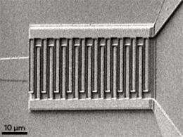
Plasmonic resonances can easily enhance the sensitivity of this light detection. The researchers introduced plasmons by adding thin aluminum contacts on top of the device (pictured). The plasmonic effects in the metal films channel considerably more light from the silicon waveguide into the photodetector, with important implications for device performance. “The enhanced photodetection enables the use of smaller devices, which in turn means that the device speed can be increased considerably,” explains Lo.
The researchers demonstrate detection speeds of 37.6 picoseconds or faster, corresponding to a data transmission speed of 11.4 gigahertz—several orders of magnitude faster than that achievable by current broadband connections.
At the same time, these speeds still lag behind the full potential of these detectors. One of the reasons, says Lo, is loss that arises from the plasmonic resonances, which absorb some of the light and therefore reduce the amount of light that arrives at the detector. “The response of the detector is lower than what we expected from our design,” says Lo. “Enhancing the plasmonic properties of the detector, for example through the design of different geometries, could alleviate such problems and enable a further miniaturization of photodetectors on silicon chips.”
The A*STAR-affiliated researchers contributing to this research are from the Institute of Microelectronics
More information: Ren, F.-F. et al. Surface plasmon enhanced responsivity in a waveguided germanium metal-semiconductor-metal photodetector. Applied Physics Letters 97, 091102 (2010). dx.doi.org/10.1063/1.3485064
Provided by Agency for Science, Technology and Research (A*STAR)


