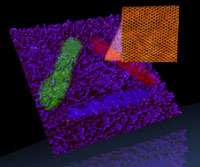
Highlight: Nanopatterning of Graphene

Center for Nanoscale Materials (CNM) at Argonne National Laboratory users from Politecnico di Milano in Italy, working collaboratively with researchers in the Electronic & Magnetic Materials & Devices Group, have demonstrated the reversible and local modification of the electronic properties of graphene by hydrogen passivation and subsequent electron-stimulated hydrogen desorption with a scanning tunneling microscope (STM) tip.
Graphene is a nearly ideal two-dimensional conductor consisting of a single sheet of hexagonally packed carbon atoms. The hydrogen passivation modifies graphene’s electronic properties, opening a gap in the local density of states.
The insulating state is reversed by local desorption of the hydrogen, upon which the unaltered electronic properties are recovered. Using this mechanism, graphene patterns can be “written” on nanometer length scales. For patterned regions 20 nm or greater, the inherent electronic properties of graphene are completely recovered. Below 20 nm, dramatic variations in the electronic properties are observed.
This reversible and local mechanism has far-reaching implications for nanoscale circuitry fabricated from this revolutionary material.
More information: P. Sessi, J. R. Guest, M. Bode, N. P. Guisinger, Nano Letters, 9, 4343 (2009).
Provided by Argonne National Laboratory


