Fujitsu Develops Power-Saving CMOS Technology for 32nm-Generation and Beyond

(PhysOrg.com) -- Fujitsu Laboratories announced today the development of power-saving CMOS technology for logic LSI chips for 32 nanometer- (32nm-) generation and beyond. The new technology enables employment of a specific silicon crystal surface, which previously had not been applied in silicon substrates due to the crystal surface's conventionally low performance in the past, by improving its performance.
As a result, as a world's first, the technology makes it possible to use current 45nm-generation fabrication facilities to reduce LSI power voltage without lowering operation speed, thereby containing production costs and cutting LSI power consumption during operation by approximately 20 percent (20%). It is anticipated that the technology can be used in a wide range of applications, such as system LSIs for various mobile devices that will need to be increasingly multi-functional, and for microprocessors of which many are running with multiple processing cores.

Details of the technology were presented at the 2008 IEEE International Electron Devices Meeting (IEDM) being held from December 15 to 17 in San Francisco.
While the functionality of mobile devices and the performance speed of servers continue to advance, rise in power consumption has been an ongoing issue. For power-saving in logic LSIs, one effective measure is reduction of power voltage. However, simply reducing the power voltage will reduce the "on-current" flow through a MOS transistor, causing a drop in operating speed. Thus, there is a need for technology capable of maintaining on-current even when power voltage is lowered. There have been attempts to address this issue through various strain technologies, but improvements in strain technologies are considered to have reached their limit with the 45nm-generation for LSIs.
Among the potential technologies for achieving higher on-current for a given voltage in the 32-nm generation and beyond are high-k technology and metal gate technology. There is also active research underway on how changes in the crystal plane of substrate surfaces can increase on-current, as electrical characteristics of a substrate surface change depending on which crystal plane of silicon is applied to a substrate surface.
Currently, the surface of silicon substrates is most commonly the high-mobility (001) surface of an NMOS transistor. However, it is difficult to increase the on-current of a (001) surface using existing 45nm-generation fabrication facilities. As an alternative, (110) surfaces have become the focus of increasing attention as they offer higher mobility than (001) surfaces when used with PMOS transistors; however, (110) surfaces have the problem of lower mobility of NMOS (110) compared to (001) surfaces. Since the combined total of NMOS on-current and PMOS on-current is higher with a (001) surface, the (110) surface had not been used as a substrate. For practical use of a (110) surface in a power-saving logic LSI, the surface would need to entail minimal increases in fabrication costs and maintain an on-current equivalent to that with NMOS on a (001) surface.
As a world's first, Fujitsu Laboratories developed new technology for 32nm-generation LSIs that can be used with existing 45nm-generation fabrication facilities using a (110) silicon substrate to enable increase in PMOS on-current, with no drop in NMOS on-current, in comparison with a (001) surface.
1. Silicon surface-treatment technology
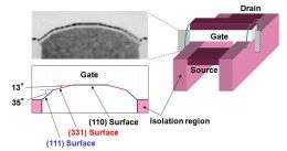
Thermal treatment applied prior to forming the gate-insulating layer changes the shape of the boundary between the silicon and the gate-insulating layer. Thermal treatment in the presence of special gases other than those normally used results in the formation of a (111) surface and (331) surface near the isolation region(7).
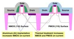
NMOS mobility in the (111) and (331) surface was greater than in the (110) surface, and while the center of the gate is still a (110) surface, overall on-current is increased by 10%. At the same time, because of the increase in mobility, PMOS on-current rises by10%.
2. Aluminum (Al) implantation into silicide
Fujitsu Laboratories discovered that implanting aluminum after forming silicide reduces contact resistance between NMOS silicide and silicon. Implanting aluminum into the ultra-shallow silicide region increases NMOS on-current by 20%. Combining this with silicon surface-treatment technology makes it possible to use a (110) silicon substrate to achieve NMOS on-current levels equivalent to those on a (001) surface.
However, it was found that PMOS contact resistance increases with the implantation of aluminum, causing a drop in PMOS on-current. Therefore, a process is added in which aluminum is selectively implanted into NMOS regions, thereby avoiding the problem of reducing PMOS on-current.
By applying this new technology to prototype chips made using (110) surface silicon substrate, compared to conventional (001) surface silicon substrate, Fujitsu Laboratories was able to increase PMOS on-current by 40% while maintaining NMOS on-current. This indicates that power voltage can be reduced by 10% without lowering operating speed, thus enabling a cut in power consumption of approximately 20%.
NMOS mobility in the (111) and (331) surface was greater than in the (110) surface, and while the center of the gate is still a (110) surface, overall on-current is increased by 10%. At the same time, because of the increase in mobility, PMOS on-current rises by10%.
Deploying this technology in existing 45nm-generation fabrication processes would require only two additional processes: thermal treatment and ion implantation. Furthermore, adopting this technology for 32nm-generation fabrication processes would result in a cost increase of just 1%, excluding wafer costs.
Provided by Fujitsu


