Samsung Says 3D Silicon Will Drive Boundless Industry Growth in Unprecedented Era of Fusion Technology
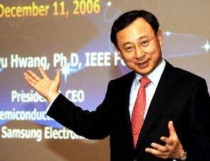
Samsung Electronics today shared stunning prospects for a new industry-fusing technology era that will offer tremendous global opportunities for expanded use of three-dimensional (3D) silicon-based technologies. At the plenary session of the 2006 International Electron Devices Meeting, Dr. Chang-Gyu Hwang, president and CEO of Samsung Electronics' Semiconductor Business, said that we are at the doorstep of the largest shift in the semiconductor industry ever, one that will dwarf the PC and even the consumer electronics eras.
In his keynote speech entitled, ‘New Paradigms in the Silicon Industry', Dr. Hwang told 3,000 professionals in the field of device technology at the Hilton San Francisco Hotel, “The approaching era of electronics technology advancement – the Fusion Era – will be massive in scope, encompassing the fields of information technology, bio-technology, and nano-technology and will create boundless opportunities for new growth to the semiconductor industry.”.
Evolving from the PC industry, which holds an annual market volume of 200 million units, the mobile and digital consumer industry now has a volume exceeding two billion units annually. In the approaching Fusion Era, market demand will soar to a level that could match the 6.5-billion world population total, with multiple applications affecting literally everyone.
While demand for semiconductor technology has been surging since 2000 for mobile, digital consumer and entertainment applications, Dr. Hwang enumerated reasons for a new, massive, and prolonged surge that Samsung anticipates will begin around 2010 and go well beyond.
Bio-tech, health care, robotics, aerospace, solar cell, and environment-friendly R&D fields are expected to combine in critical ways to herald the dawning of the New Era of Fusion Technology. Semiconductor advancements will play a pivotal role in enabling this new trend, Dr. Hwang said.
“Unlike the paradigm shift from the personal computer to mobile and digital consumer applications, the introduction of massive-scale fusion technology – which represents the organic convergence of IT, BT and NT, will bring together a wide range of technology-related professions as the foundation for a new technology frontier,” Dr. Hwang said. “This historic new frontier will change the way we develop and harness semiconductor technologies in substantially improving the level of day-to-day convenience for consumers.”
Commencement of the Fusion Era depends on the successful development of high-density, ultra-small, multi-featured semiconductor chips and multi-faceted, cross-industry solutions. To enter the new era, Dr. Hwang said it is essential to first overcome today's limits in nano-technology.
In blending critical aspects of key semiconductor technologies for a sweeping technology migration, Dr. Hwang also cautioned that multiple hurdles need to be overcome, such as moving beyond today's silicon patterning limitations, ensuring controllability of limited sums of electrons, and minimizing inter-cell noise that has caused bottlenecks in two-dimensional structures.
To resolve such technology limitations, a promising 3D approach has already been made to transistor design. However, further innovations in the design of architecture for electronics components and more efficient use of raw materials are critical to achieving additional advancements that will pave the way to the new era.
Today, it is generally perceived that sub-25 nanometers is the limit to maximizing the efficiency of the silicon base. But, Dr. Hwang emphasized that alternate technologies can counter this apparent dead-end in ultra-fine process technology such as 3D structure technology and 3D stacking technology.
Shedding more light on how hurdles to the Fusion Era will be overcome, Dr. Hwang said that Samsung is presenting two papers on 3D silicon wire technology at the IEDM 2006 technology sessions that represent critical advancements in enabling ultra-fine process technology with a wire diameter of five nanometers.
Another highly significant paper being presented by Samsung at IEDM 2006 focuses on the development of NAND flash memory based on charge trap flash (CTF) technology, which Dr. Hwang said, will be the basis for producing 32-gigabit NAND memory in the near future using 40-nanometer process technology as announced in September.
Regardless of such breakthroughs in high-density, scaled memory technology, the common perception has been that sub-25-nanometer would be the limit for silicon-based chip production. However, research engineers are continuing to challenge these apparent barriers in the pursuit of new fields such as bio technology and various molecular-level technologies.
Along with accelerated research on baseline technologies, Dr. Hwang said that Samsung continues to expend considerable resources on the development and refinement of fusion semiconductors. First introduced in 2002, Samsung's fusion semiconductors have converged multiple device characteristics onto a single piece of silicon.
The first fusion memory, OneNAND TM , has been widely adapted to mobile applications from handsets and removable memory cards to hard disk drives. Today, Samsung is announcing a second generation of fusion memory – the OneDRAM TM . This new fusion memory chip will offer better performance, with faster speed and lower power consumption and a lower chip count, with reduced area coverage on the printed circuit board. As the second generation in fusion memory, OneDRAM enhances performance in mobile applications with data processing speeds up to five times faster than conventional data transfer methods used today.
To launch the Fusion Era, high-density semiconductors on a terabit scale are expected by 2010, moving later to even higher densities on the peta scale, Dr. Hwang said. The core element needed to usher in the new age will be a complex integration of different types of devices such as memory, logic, sensor, processor and software, together with new materials, and advanced die stack technologies, all based on 3D silicon technology, he added.
Source: Samsung Electronics


