Applied Materials Launches Black Diamond II Low k Solution for Next Generation High-Speed Chips
Applied Materials, Inc., the worldwide market leader in low k dielectric film technology, today announced its new Applied Producer Black Diamond II system for depositing the semiconductor industry's most advanced low k film. Providing a k-value of less than 2.5, the Black Diamond II system utilizes Applied's innovative NanoCure UV curing technology to achieve a robust, manufacturable film compatible with CMP and packaging processes.
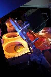
Image: The new Applied Producer Black Diamond II system deposits the industry's most advanced low k film, providing a k-value of less than 2.5.
Black Diamond II enables the continued scaling of copper/low k interconnects to 45nm and beyond -- allowing chipmakers to create faster, more powerful devices that will drive next-generation mobile electronics and computers.
"The Applied Producer Black Diamond II system overcomes the significant technical challenges of integrating low k films for the 45nm node and beyond, while delivering the reliability customers require for volume production," said Dr. Farhad Moghadam, senior vice president and general manager of Applied Materials' Thin Films Product Business Group. "A number of key customers in the U.S., Taiwan, and Europe, as well as influential development organizations like IMEC, are designing Black Diamond II into their most advanced, highest-performance chips. Our depth of experience with low k technology offers chipmakers a wealth of knowledge to accelerate the critical integration process in fabricating advanced low k interconnects."
The Applied Black Diamond II system builds on the company's award-winning Black Diamond technology, combining advanced low k CVD(1) with its new NanoCure UV chamber on the high-productivity Producer platform to achieve the critical properties required for advanced interconnects. Key to the film's low k-value is its tightly distributed small-sized pores, which provide excellent integration stability and high mechanical integrity.
Applied's NanoCure process is the only UV cure available today that provides in situ cleaning -- an important requirement to achieve high uptime and low defects. The NanoCure chamber is available to customers on the Producer platform, either integrated with the Applied Black Diamond II chamber or in a stand-alone configuration for greater fab flexibility. For more information on this system, please visit www.appliedmaterials.com/produ … nd.html?menuID=1_4_3 (Due to its length, this URL may need to be copied/pasted into your Internet browser's address field. Remove the extra space if one exists.)


