Fujitsu Develops Breakthrough Technology for Low-Cost Production of Gallium-Nitride HEMT
Reduces production costs to less than 1/3
Fujitsu Laboratories Ltd. today announced the development of a technology that enables low-cost production of gallium-nitride (GaN)(1) high electron mobility transistors (HEMT)(2), a key technology in mobile base station amplifiers for 3G and beyond. This breakthrough technology reduces GaN HEMT production costs to less than one-third that of conventional levels, thereby contributing to the realization of lower-cost GaN HEMT-based amplifiers.
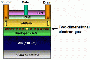
Cross section of newly developed GaN HEMT
The technology is designed to enable practical use of compact, more energy-efficient mobile base stations using GaN HEMT.
Details of this technology were presented at the International Electron Device Meeting (IEDM) 2004 held in San Francisco last week.
Background
Because they can be driven at high voltages with excellent output performance and efficiency, there is much anticipation for GaN HEMT amplifiers that can be used as high-output amplifiers suitable for the next generation of mobile base stations. Fujitsu has verified that amplifiers using its proprietary GaN HEMT technology in combination with its distortion compensation circuits(3) can achieve superior efficiency and output levels for use in 3G and future generations of mobile base stations. However, there was a need to develop technology that enables low-cost production of GaN HEMT, in order for volume production and commercialization.
Technological Challenges
Fujitsu has been using semi-insulating silicon carbide (SiC) substrates in past GaN HEMT it has developed. Although GaN-HEMT using semi-insulating SiC is able to reliably deliver high operating efficiency compared to other materials, semi-insulating SiC is expensive and therefore becomes a factor that increases production costs for GaN HEMT. Fujitsu has been researching the use of low-cost conductive SiC substrates(4), which are less expensive than semi-insulating SiC substrates and which have already been commercialized for practical use in applications such as blue LEDs. However, technological issues to overcome for practical application of conductive SiC substrate were that parasitic capacitance(5) between an electrode pad and a conductive SiC substrate leads to lower gain(6), and increase of current leakage to the conductive SiC substrate.
Fujitsu's New Technology
Fujitsu's newly developed technology is a breakthrough for low-cost manufacturing of GaN HEMT. This was achieved by forming an aluminum nitride (AlN) epitaxial layer of 10 micrometers or more on the conductive n-type SiC substrate, followed by an epitaxial layer of GaN HEMT developed on top of this substrate.
Fujitsu discovered that by simulating the effect of the AIN thickness on gain, parasitic capacitance could be decreased when AIN thickness was more than 10 micrometers. As a result, high gain was successfully achieved as predicted. AIN was grown on a n-SiC using hydride vapor phase epitaxy(7) and GaN HEMT was grown on AIN using metal organic vapor phase epitaxy(8).
Furthermore, by using AIN, which features a wider band gap(9) than GaN, and by optimizing GaN growth conditions on AIN, Fujitsu succeeded in suppressing leakage current to the conductive substrate.
Results
Fujitsu's breakthrough technology reduces production cost of GaN HEMT to less than one-third that of conventional levels by using conductive SiC substrates which are more economical than semi-insulating silicon carbide (SiC) substrates, thereby making it possible to manufacture low-cost GaN HEMT amplifiers.
Fujitsu successfully achieved characteristics sufficient for practical application of GaN HEMT amplifiers, including maximum output of 101 watt, maximum power-added efficiency(10) of 50%, and gain of 15.5 decibels.
Future Developments
Fujitsu plans to apply this low-cost production technology for GaN HEMT to its manufacturing processes, with commercial application targeted for within the next one to two years.
Glossary
(1) gallium-nitride (GaN): A type of wide band-gap semiconductor that is more resistant to breakdown at a given voltage than conventional semiconductors, such as gallium arsenide and silicon.
(2) high electron mobility transistors (HEMT): A field-effect transistor that takes advantage of operation of the electron layer at the boundary between different semiconductor materials that is relatively rapid compared to that within conventional semiconductors. Fujitsu led the industry with its development of HEMT technology in 1980, and the technology now underpins much of today's fundamental IT infrastructure, including satellite transceivers, wireless equipment, GPS-based navigation systems, and broadband wireless networking systems.
(3) distortion compensation circuits: Fujitsu's distortion compensation technology is based on the Digital Pre-Distortion (DPD) method, which adds compensatory characteristics to the signal before distortion occurs. Fujitsu has incorporated this technology into a distortion-compensation chip.
(4) low-cost conductive SiC substrates: Low resistance SiC substrate that is easy to produce, thereby resulting in low cost compared with S.I. SiC substrate.
(5) parasitic capacitance: Capacitance that does not result from a device's active region during operation. When using a conductive substrate, capacitance may occur between the substrate and an electrical contact. Because this parasitic capacitance can degrade high-frequency characteristics, it is mandatory that parasitic capacitance be minimized.
(6) gain: The ratio between an input signal and output signal in an amplifier, indicating the conversion efficiency of output power as input power.
(7) hydride vapor phase epitaxy: A high-temperature method of forming an epitaxial layer that uses aluminum chloride and ammonia as source materials. Epitaxial AlN layers were grown using aluminum-chloride and ammonia at a high temperature.
(8) metal organic vapor phase epitaxy: A high-temperature method of forming an epitaxial layer that uses alkyl-aluminum, alkyl-gallium, and ammonia as source materials.
(9) band gap: The energy band in which electrons in a semiconductor crystal cannot exist. Because atoms in a semiconductor crystal are adjacent, their action on one another causes electrons to pass energy continuously. However, an energy band (the band gap) can be formed such that electrons cannot occupy that state in the passage of energy. Semiconductors for which this band gap is large are known as wide band-gap semiconductors.
(10) maximum power-added efficiency: A ratio indicating the conversion efficiency of direct current as an output signal supplied to an amplifier, converted to high-frequency power.


