Breaking Barriers, NC State Engineers Patent Methods for Creating Self-Assembling, 3-D Nanostructures
Nanotechnology promises to revolutionize modern life. From energy-efficient lighting that lasts for 50 years, to greater data storage capacity, to stronger metals and ceramics, the improvements attributed to the development of nanostructures seem limitless. So far, the greatest impediment to developing these advances has been creating usable nanostructures that self-assemble. Engineers at North Carolina State University recently applied for a patent for two processes that help break that barrier.
Dr. Jagdish “Jay” Narayan, the John C.C. Fan Family Distinguished Professor of Materials Science and Engineering and director of the NSF Center for Advanced Materials and Smart Structures at NC State, and Dr. Ashutosh Tiwari, research associate in the Department of Materials Science and Engineering, developed two methods for self-assembly of three-dimensional nanostructures.
Results of their research will be published in the September issue of the Journal of Nanoscience and Nanotechnology with images of the newly created structures appearing on the cover of the journal. The research was supported in part by the National Science Foundation (NSF).
The new methods are a breakthrough in nanotechnology that opens the door to creating new materials for a myriad of applications, including super-dense data storage, solid-state lighting, super-strong materials and advanced detection systems. According to Narayan, three-dimensional self-assembly is the key to being able to use the nanostructures.
“The grand challenge is to be able to use the nanounit in the form of nanodot, nanowire or nanodisc,” said Narayan. “In the past we could make only one layer of the nanostructure with these units. There was only two-dimensional self-assembly, which is not usable for applications. We couldn’t control the properties of the medium. Now, with this development, we can control the medium and do three-dimensional self-organization. More importantly, we can change the size in different layers and change the functionality at different depths.”
“National Nanotechnology Initiative (NNI) has created a broad base of scientific discovery and potential technological development,” said Dr. Mihail Roco, senior advisor for nanotechnology at NSF and chair of the NNI organization. “This research shows the importance of creating infrastructure because NC State University has established a strength in the area of nanostructured materials, and at this moment, we can see several results that weren’t initially planned.”
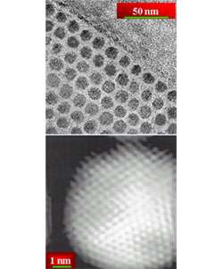
The two methods involve using pulsed laser deposition, which works with a variety of materials and reduces imperfections. The sequential growth method uses the laser pulses to ablate successive targets to create layers of nanodots in a matrix. The simultaneous growth method is based on the difference in the oxidation rate of the nanodot and matrix materials. In this method the matrix and nanodots are deposited simultaneously on a substrate. Both methods produce consistent size and shape of the nanodots and demonstrate control of the materials that cannot be achieved by previously proposed methods.
“This device is part of the first generation of passive nanostructures which illustrate how one can exploit new phenomena and behavior of materials at the nanoscale for economic advantage,” said Roco.
The patented processes can be applied to almost any material. To create nanostructures for the different applications, the material used for the nanodots and the matrix are changed. For example, to create structures for data storage, Narayan uses nickel; for solid-state applications, gallium nitride or zinc oxide is used; for super-strong materials, copper, tungsten carbide and nickel aluminide are used; and for ceramics, aluminum oxide is used.
The most interesting application may be the development of energy-efficient, low-cost, solid-state lighting. By creating a matrix of layers of varying sizes of nanodots embedded in a transparent medium such as aluminum oxide, Narayan can create a chip that glows with white light. Solid-state lighting would use about one-fifth the energy of standard fluorescent lighting and last for approximately 50 years.
Another interesting application for the nanodots is the development of a chip that can hold 10 terabits of information – information that equals 10 million million or 10 to the 13th power bits – which is equivalent to 250 million pages of information. Narayan estimates that a chip with this storage capacity represents an increase of more than two orders of magnitude, in fact, or five hundred times the existing storage density available today.
According to Narayan, the key to moving nanotechnology from the laboratory to the consumer is keeping the cost of manufacturing low because people will not embrace a new technology if the cost is substantial. He believes that the beauty of these new processes is that they make it possible to build a three-dimensional matrix of nanodots that is not only more efficient but also costs less to produce. Using Narayan’s methods, all of the steps can be performed in the same processing chamber, reducing the manufacturing cost and the impact on the environment.
With further development of these new processes, copper can be created that is as strong as steel, and ceramics can be made tough enough to be used in automobile engines. The major difficulty with most materials is the problem of defects. However, when materials are reduced in size to nanoscale, the defects are reduced or eliminated, creating stronger materials that would last much longer and be less likely to fail. For example, ceramics are excellent performers at high temperatures but are currently too brittle to be used in automobile engines. Applying nanotechnology would create a ceramic material that would be able to withstand the stress that affects an automobile engine. Because ceramics perform at higher temperatures, a ceramic automobile engine could run at a higher temperature and thus run more efficiently – essentially creating a more fuel-efficient vehicle.
Other applications include spin transistors and single electron transistors. Since these new methods can create self-assembled matrices of nanodots both randomly and epitaxially, the applications are seemingly infinite. The random self-assembly method is most cost effective and would be used for storage applications. The more expensive epitaxial self-assembly method would be used to create spin transistors that use less power because heat losses are reduced or eliminated.
Narayan anticipates that the first applications of his nanodots will be available to consumers within the next five years. He predicts that data storage and solid-state lighting will be the most likely consumer applications to be developed during that time.
Source: NC State University


